Cascode amplifier is a two-stage circuit consisting of a transconductance amplifier followed by a buffer amplifier. The word “cascade” was originated from the phrase “cascade to cathode”. This circuit has a lot of advantages over the single-stage amplifier like better input-output isolation, better gain, improved bandwidth, higher input impedance, higher output impedance, better stability, higher slew rate, etc. The reason behind the increase in bandwidth is the reduction of the Miller effect. Cascode amplifier is generally constructed using FET ( field effect transistor) or BJT ( bipolar junction transistor). One stage will be usually wired in the common source/common emitter mode and the other stage will be wired in common base/ common emitter mode.
Miller effect.
Miller effect is actually the multiplication of the drain to source stray capacitance by the voltage gain. The drain to source stray capacitance always reduces the bandwidth and when it gets multiplied by the voltage gain the situation is made further worse. Multiplication of stray capacitance increases the effective input capacitance and as we know, for an amplifier, the increase in input capacitance increases the lower cut off frequency and that means reduced bandwidth. The Miller effect can be reduced by adding a current buffer stage at the output of the amplifier or by adding a voltage buffer stage before the input.
FET Cascode amplifier.
The circuit diagram of a typical Cascode amplifier using FET is shown above. The input stage of the circuit is an FET common source amplifier and the input voltage (Vin) is applied to its gate. The output stage is an FET common gate amplifier which is driven by the input stage. Rd is the drain resistance of the output stage. Output voltage (Vout) is taken from the drain terminal of Q2. Since the gate of Q2 is grounded, FET Q2’s source voltage and the FET Q1’s drain voltage are held almost constant. That means the upper FET Q2 offers a low input resistance to the lower FET Q1. This reduces the gain of lower FET Q1 and as a result the Miller effect also gets reduced which results in increased bandwidth. The reduction in gain of the lower FET Q1 does not affect the overall gain because the upper FET Q2 compensates it. The upper FET Q2 is not affected by the Miller effect because the charging and discharging of the drain to source stray capacitance is carried out through the drain resistor and the load and the frequency response if affected only for high frequencies (well over the audio range).
In Cascode configuration, the output is well isolated from the input. Q1 has almost constant voltage at the drain and source terminals while Q2 has almost constant voltage at its source and gate terminals and practically there is nothing to feed back from the output to input. The only points with importance in terms of voltage are the input and output terminals and they are well isolated by a central connection of constant voltage.
Practical Cascode amplifier circuit.
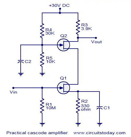
A practical Cascode amplifier circuit based on FET is shown above. Resistors R4 and R5 form a voltage divider biasing network for the FET Q2. R3 is the drain resistor for Q2 and it limits the drain current. R2 is the source resistor of Q1 and C1 is its by-pass capacitor. R1 ensures zero voltage at the gate of Q1 during zero signal condition.


Cascode Amplifier >>>>> Download Now
ReplyDelete>>>>> Download Full
Cascode Amplifier >>>>> Download LINK
>>>>> Download Now
Cascode Amplifier >>>>> Download Full
>>>>> Download LINK ui